The demand for high-performance computing driven by AI is insatiable. However, when the number of transistors integrated per unit volume reaches physical limits, alternative solutions must be found to sustain its scalability.
So, where do we look next? The answer lies in technologies such as heterogeneous integration, advanced packaging, and chiplets. These emerging technologies are quietly revolutionizing the semiconductor manufacturing industry, presenting new opportunities and challenges. Heterogeneous integration allows the integration of chip modules of different types and functionalities, enabling higher performance and efficiency. Advanced packaging technologies enable multiple chips to be packaged together to form a larger chip, thereby enhancing computational power.
The application of technologies like heterogeneous integration, advanced packaging, and chiplets will inject new vitality into the semiconductor manufacturing industry and further drive the advancement of technologies such as artificial intelligence.
Chip and Packaging Technology Challenges
Facing the challenges posed by physical limits and the urgent demand for high-performance computing, heterogeneous integration and advanced packaging technologies have emerged. If we conceptualize the integration of transistor count per unit volume as Vertical (vertical development), heterogeneous integration represents Horizontal (horizontal development). This approach allows for broader lateral expansion and the integration of multiple chips to compensate for the limitations in transistor count per individual chip.
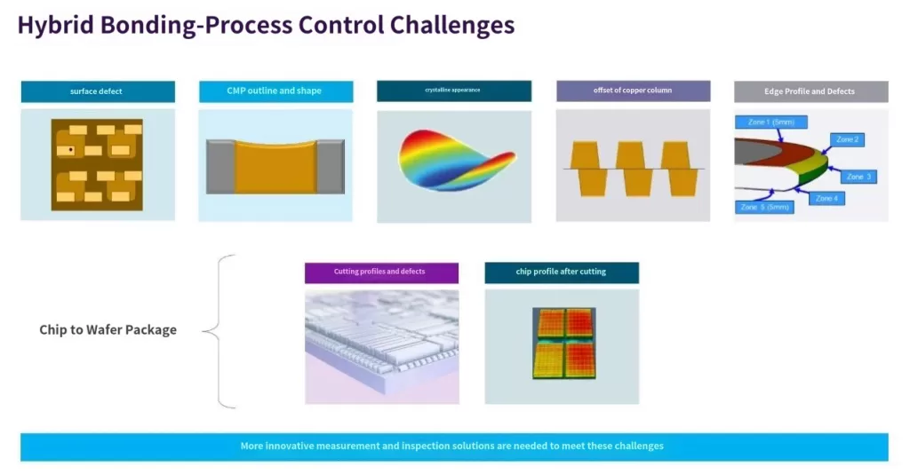
Heterogeneous integration effectively extends the scalability requirements of high-performance computing. However, the actual manufacturing process is not without its challenges, which is why it remains a current hot topic. Simply combining multiple chips into a single package is not cutting-edge technology. Integrating all cutting-edge chips into one unit and ensuring their performance increases several times over seems straightforward but actually relies on sacrificing some yield to achieve limited gains. This is mainly due to the challenges posed by new manufacturing processes, new materials, and the mixed application of front-end (FE) and back-end (BE) processes (as shown in Figure 1). While this manufacturing process can sustain Moore’s Law in terms of performance, it also brings more challenges in manufacturing and yield (Figure 2).


The challenge posed by increasing bumping density: As lateral expansion enhances the number of chips per unit area, the next step involves addressing the matching chip-to-chip transfer rates. Advanced packaging solutions, such as the mixed bonding bumping process, offer a solution to this issue. The spacing between bumpings is shrinking (Figure 3). While this packaging technology enables shorter interconnection paths and more connections between chips, interconnecting Known Good Dies (KGDs) is not straightforward. Particularly in the current evolving state of heterogeneous integration manufacturing ecosystems, there is a need for more reliable process control and yield management solutions to support stable mass production. Mixed bonding has become a critical turning point for heterogeneous integration.

Control solutions for chip and advanced packaging processes
Heterogeneous integration and advanced packaging’s mixed bonding process are key technologies for expanding various packaging types and applications. The primary advantage of mixed bonding is enhancing speed, bandwidth, and power efficiency by increasing interconnect density. W2W (wafer-to-wafer) integration in mixed bonding is critical for manufacturing CMOS image sensors and 3D NAND, while D2W (die-to-wafer) integration is commonly used for AI logic chips and high-bandwidth memories. These complex processes across various stages pose significant challenges to final yield of the products. Ensuring high final yield and enabling mass production requires crucial process control and yield management tools. KLA provides professional manufacturing, inspection, and metrology solutions that have been extensively validated by the industry (Figure 4).

Conclusion
If the high-performance computing demands of artificial intelligence are driving the wave of heterogeneous integration and advanced packaging, overcoming yield and capacity challenges becomes an indispensable part of KLA’s innovative technology development. We can envision the costly scrapping of multi-chip packages or additional screening due to defects in an integrated chip, which is unacceptable. KLA is dedicated to developing comprehensive packaging process solutions, including:
- Process solutions: Ensuring yield during manufacturing processes.
- Metrology solutions: Quantitative analysis and control of production process variations, ensuring process errors are always within specification for new products and mass production.
- Inspection solutions: Effectively managing yield for each in-process product, ensuring long-term controllable final yields.
KLA combines these capabilities with extensive yield management, inspection, and metrology systems, aiming to be the ideal partner for advanced packaging manufacturers.


